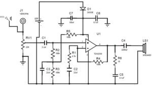
2030 IC Circuit Diagram
What is an IC TDA 2030? What is a 2030 IC? Is it a new technology? Is it a new concept?
Overview of TDA 2030 and its features, functions, and capabilities. Overview of TDA 2030 background, history, and evolution. Overview of TDA 2030 architecture and main components. Overview of TDA 2030 subsystems and functions.
To design the audio amplifier circuit, the IC TDA2030 is the best choice. Because this IC is inexpensive, very simple to utilize, and apt for electronic beginners, it is one of the most commonly used IC in audio circuit design. In this part, I’ll introduce you to the audio amplifier circuit using the IC TDA2030. I’ll also show you some of the applications of this IC.
TDA2030 IC Features
- This is suitable for the amplification of audio
- The output power of this IC is up to 20 Watts
- The power supply range is wide from 6V- 36V
- Thermal & short circuit protection is available
- It is obtainable in the package of 5 pin
- The maximum voltage supply is +/- 18VDC
- The minimum voltage supply is +/- 6VDC
- The power driver outputs at 4Ω are 14W & at 8Ω is 9W
- The maximum current is 900mA
- The frequency response range at -3dB is 10HZ to 140KHz
TDA 2030 IC Pinout

TDA 2030 IC Pin Diagram
IC TDA2030 of pin configuration is given below.
- Pin1 (Non-Inverting Input): This pin is the Positive terminal of the amplifier
- Pin2 (Inverting Input): This pin is the negative terminal of the amplifier
- Pin3 (Vs): This pin connects to the ground terminal
- Pin4 (Output): This pin generates the amplified signal
- Pin5 (Vs): This is a supply voltage pin that generates min 6V & Max 36V.
TDA2030 is a monolithic linear integrated circuit in the Pentawatt package, designed for use as an audio class AB amplifier. It has low harmonic distortion, low noise, and very good output accuracy. It can deliver up to 14W into a 4Ω load and operates from a single power supply voltage.
Here are a few more details about the TDA2030 amplifier:
- The TDA2030 is a classic analog linear amplifier and is widely used in DIY audio projects.
- It has high input impedance, which makes it suitable for use with low output impedance sources, such as a preamp or a CD player.
- The TDA2030 can be used in bridge mode, which can result in a power increase of up to four times compared to a single-ended operation.
- It features internal thermal overload protection and short circuit protection, making it relatively safe to use.
- The TDA2030 is pin-compatible with several other similar linear amplifier ICs, including the TDA2050 and TDA2040, making it easy to upgrade or replace in existing designs.
TDA2030 IC Amplifier Circuit Diagram

2030 IC Circuit Diagram
In this circuit, the required components used in the TDA2030 IC subwoofer circuit are an audio jack pin, IC TDA2030 IC, Resistors three-100K, one- 4.7 K, and one 0 ohm, capacitors like one-100mf, two-0.1mf, two-2.2mf & one-22mf, one- In4007 diode, one speaker, 12v battery, and one variable resistor with 22k value.
The TDA2030 IC subwoofer circuit using 12v is shown above. A 2.2uf capacitor is connected in series with a noninverting pin of the IC and it acts like HPF (high pass filter). The main function of this filter in this amplifier is to allow high-frequency audio signals.
The R4 resistor which is connected between pins 2 and 4 is known as a feedback resistor, the connection of R1 and C2 can be done in series. Through pin 2 of the IC, it holds back the noises within the audio signal, and pin 3 is grounded. The output of the IC is connected through the 2200uf value of the series capacitor.
TDA2030 IC Applications
- Used in high-power amplification
- It operates on a Dual or Split power supply
- It is used in audio speakers for cascading
- In amplifying audio signals
2030 IC Datasheet Pdf Download
Tda2030 Datasheet Download – Tda2030 Datasheet pdf Click Here
